- 您现在的位置:买卖IC网 > Sheet目录251 > SFCF64GBH2BU4TO-I-NU-517-STD (Swissbit NA Inc)FLASH SLC UDMA/MDMA/PIO 64GB
8.4 I/O Primary and Secondary Address Configurations
When the system decodes the Primary and Secondary Address Configurations, the registers are accessed in the
Address A0 must be low for all word accesses. As for the Memory Mapped Addressing, register 0 is accessed with –
CE1 Low and – CE2 Low (A0 must be 0) as a Word register on the combined Odd and Even Data Bus (D15 to D0). This
register may also be accessed with – CE1 Low and – CE2 High, by a pair of Byte accesses to offset 0. The address
space of this Word register overlaps the address space of the Error and Feature Byte-wide registers at offset 1.
When accessed twice as Byte register with – CE1 Low, the first Byte is the even Byte of the Word and the second is
the odd Byte. A Byte access to register 0 with – CE1 High and – CE2 Low accesses the error (read) or feature (write)
register.
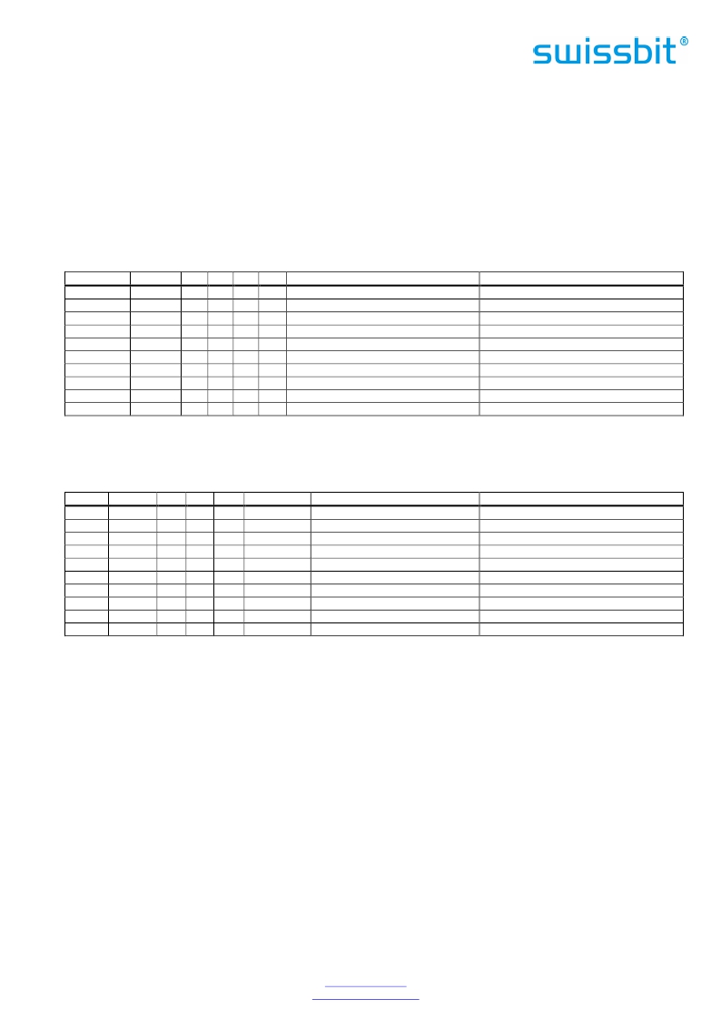
Table 45: Primary and Secondary I/O Decoding
- REG
0
0
0
0
0
0
0
0
0
0
A9 to A4
1F(17)h
1F(17)h
1F(17)h
1F(17)h
1F(17)h
1F(17)h
1F(17)h
1F(17)h
3F(37)h
3F(37)h
A3
0
0
0
0
0
0
0
0
0
0
A2
0
0
0
0
1
1
1
1
1
1
A1
0
0
1
1
0
0
1
1
1
1
A0
0
1
0
1
0
1
0
1
0
1
- IORD=0
Even Data Register
Error Register
Sector Count Register
Sector Number Register
Cylinder Low Register
Cylinder High Register
Select Card/Head Register
Status Register
Alternate Status Register
Drive Address Register
- IOWR=0
Even Data Register
Feature Register
Sector Count Register
Sector Number Register
Cylinder Low Register
Cylinder High Register
Select Card/Head Register
Command Register
Device Control Register
Reserved
8.5 True IDE Mode Addressing
Table 46: True IDE Mode I/O Decoding
- CS1
1
1
1
1
1
1
1
1
1
0
- CS0
0
1
0
0
0
0
0
0
0
1
A2
0
X
0
0
0
1
1
1
1
1
A1
0
X
0
1
1
0
0
1
1
1
A0
0
X
1
0
1
0
1
0
1
0
-DMACK
1
0
1
1
1
1
1
1
1
1
- IORD=0
PIO RD Data
DMA RD Data
Error Register
Sector Count
Sector No.
Cylinder Low
Cylinder High
Select Card/Head
Status
Alt Status
- IOWR=0
PIO WR Data
DMA WR Data
Features
Sector Count
Sector No.
Cylinder Low
Cylinder High
Select Card/Head
Command
Control Register
Swissbit AG
Industriestrasse 4
Swissbit reserves the right to change products or specifications without notice.
Revision: 1.00
CH-9552 Bronschhofen
Switzerland
www.swissbit.com
industrial@swissbit.com
C-440_data_sheet_CF-HxBU_Rev100.doc
Page 50 of 102
发布紧急采购,3分钟左右您将得到回复。
相关PDF资料
SFN08B4702CBQLF7
RES ARRAY 47K OHM 7 RES 8-DFN
SFP1050-12BG
FRONT END AC/DC 1050W 12V
SFP450-12BG
PWR SUP 450W 12V 36.6A W/STANDBY
SFSD1024N1BN1TO-I-DF-151-STD
FLASH MICRO SD CARD IND S-200 1G
SFSD2048L1BN2TO-I-DF-151-STD
FLASH SECURE DGTL CARD SD 2G
SFSD4096L1BN2TO-I-Q2-141-STD
FLASH SECURE DGTL CARD SDHC 4G
SFSD8192N1BW1MT-E-QG-111-STD
FLASH MICRO SD 8GB EXT TEMP
SFUI4096J1BP2TO-I-DT-211-STD
FLASH DRIVE USB MODULE U-110 4G
相关代理商/技术参数
SFCF64GBH2BU4TO-I-NU-527-STD
制造商:SWISSBIT 功能描述:CFC C-440 DENSITY INDUSTRIAL - Trays 制造商:SWISSBIT NA INC 功能描述:FLASH CARD 64GB IND C-440 制造商:Swissbit 功能描述:Memory Cards 64GB IND COMPACT FLASH SLC NAND C440
SFCF8192H1BO2TO-C-Q1-523-SMA
制造商:SWISSBIT NA INC 功能描述:FLASH
SFCF8192H1BO2TO-C-Q1-533-ZP1
制造商:SWISSBIT NA INC 功能描述:FLASH
SFCF8192H1BO2TO-C-Q1-543-SMA
制造商:SWISSBIT NA INC 功能描述:FLASH
SFCF8192H1BO2TOIQ1523SMA
制造商:Swissbit 功能描述:Flash Card 8G-Byte 3.3V/5V CompactFlash 50-Pin
SFCF8192H1BO2TO-I-Q1-523-SMA
功能描述:FLASH SLC UDMA/MDMA/PIO 8G RoHS:是 类别:存储卡,模块 >> 存储器,PC 卡 系列:C-320 标准包装:30 系列:- 存储容量:8GB 存储器类型:存储卡 - Extreme III SD?
SFCF8192H1BO2TO-I-Q1-533-ZP1
制造商:SWISSBIT NA INC 功能描述:FLASH
SFCF8192H1BO2TO-I-Q1-543-SMA
制造商:SWISSBIT NA INC 功能描述:FLASH
